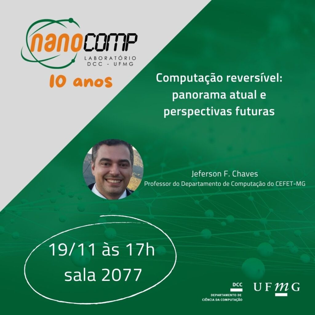
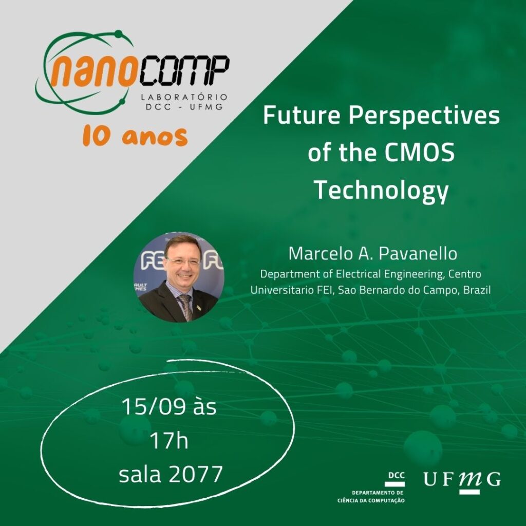
Na segunda-feira, 15, às 17h, na sala 2077 do Instituto de Ciências Exatas (ICEx), o professor do Departamento de Engenharia Elétrica do Centro Universitário FEI, em São Bernardo do Campo, Marcelo A. Pavanello, irá proferir a palestra “Future Perspectives of the CMOS Technology”. A palestra será a primeira de uma série, coordenada pelo professor do Departamento de Ciência da Computação (DCC) da UFMG, Omar Paranaiba Vilela Neto, em comemoração aos dez anos do Laboratório NanoComp.
Abaixo, em inglês, o resumo da palestra e a bio do professor:
The aggressive scaling of MOSFET dimensions triggered the search for alternative solutions for the traditional planar transistors for future technological nodes. Also, the advent of Quantum Computing raised interest in the cryogenic operation of ultimate MOSFETs to be applied in interface circuits between the Qubits and the electronic systems. Planar and tridimensional MOSFETs operating with fully depleted (FD) silicon fabricated in Silicon-On-Insulator (SOI) substrates are among the technological solutions being widely investigated.
Triple-gate Ω-shaped MOSFETs with fin height and width of similar dimensions, in the order of 10-15nm, commonly referred to as nanowires (NWs) in the literature, are promising contenders. More recently, stacked NWs (or nanosheets) also appeared as a viable technological alternative to increase the current density per footprint. Due to their tridimensional architecture, NWs and stacked NWs have been shown to promote improved control of the channel charges, leading to reduced short channel effects and great scalability, which results in excellent electrical properties for both digital and analog applications. Moreover, due to their nanometer-size channel, quantum transport can be evidenced in aggressively scaled nanowires at cryogenic temperatures. On the other hand, planar thin-film FD SOI MOSFETs have achieved maturity for mass production and are also considerable alternatives for Quantum Computing.
In this scenario, this talk will present and discuss the technological trends for the future of CMOS technology, from planar MOSFETs to tridimensional transistors. The operation of some technological contenders for Quantum Computing exposed to cryogenic temperatures down to 4 K will be presented. Peculiarities of these devices while operating in the cryogenic regime, such as transconductance oscillations indicating carrier confinement and self-heating, will be discussed.
Short-CV
Marcelo Antonio Pavanello (S´99-M´02-SM´05) is a Full Professor at the Electrical Engineering Department of Centro Universitario FEI. His current interests are compact modeling, fabrication, electrical characterization, and simulation of SOI CMOS transistors with multiple gate configurations and silicon nanowires; the wide temperature range of operation of semiconductor devices; and the digital and analog operation of novel channel-engineered SOI devices and circuits. He is the author or co-author of more than 400 technical papers in peer-reviewed journals and conferences, and the author/editor of 6 books. Dr. Pavanello is an A-Level Researcher Associated with the National Council for Scientific Development (CNPq), Brazil, a Senior Member of the IEEE, and a member of the Brazilian Microelectronics Society. Since 2019, he has been an Editor of IEEE Transactions on Electron Devices. Since 2021, he has been an Editor of the IEEE Access journal. Since 2007, he has served as IEEE Electron Devices Society (EDS) Distinguished Lecturer and has been nominated to the Compact Modeling Technical Committee (CMTC) of EDS between 2018 and 2021. In 2008, he was with UCL as a visiting professor. Between 2010 and 2020, he also served as Vice-Rector for Teaching and Research at FEI. Dr. Pavanello coordinates several research projects fomented by Brazilian agencies like FAPESP, CNPq, and Capes. He also supervised several Ph.D. dissertations, MSc theses, and undergraduate projects in Electrical Engineering.
Dr. Pavanello received an Electrical Engineering degree from FEI University in 1993, receiving the award “Instituto de Engenharia” for being the best student among all the modalities of engineering programs offered at FEI. He received the M. Sc. and Ph. D. degrees in 1996 and 2000, respectively, in Electrical Engineering (Microelectronics) from the University of São Paulo, Brazil. From August to December 1998, he was with Laboratoire de Microélectronique from Université Catholique de Louvain (UCL), Belgium, working in the fabrication and electrical characterization of novel channel-engineered Silicon-On-Insulator (SOI) transistors. From 2000 to 2002, he was with the Center of Semiconductor Components and Nanotechnologies, State University of Campinas, Brazil, where he worked as a post-doctoral researcher in developing a CMOS n-well process. In 2003, he joined FEI University.